


In the systems that feature as IBM's supercomputer line, the p690 series the nodes still contain the POWER4+ chip as the computational engine although the succesor, the POWER5 chip already is available in other server lines of IBM. Undoubtly the POWER5 will eventually appear in the p690-type systems but presently this is not yet the case. So, we discuss both chips, the POWER4+ and the POWER5 as the successor that will replace it.
At the time of writing, the clock frequency of the POWER4+ is 1.5--1.9 GHz. It is a boost of the original POWER4 chip and has no new features other than the higher clock frequency. The chip size has become so large (or rather the feature size has become so small) that IBM places now two processor cores on one chip as shown in Figure 10a. The chip also harbours 1.5 MB of secondary cache divided over three modules of 0.5 MB each.
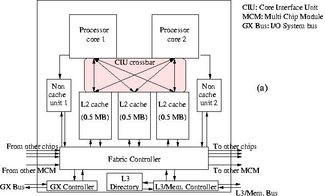
The L2 cache module are connected to the processors by the Core Interface Unit (CIU) switch, a 2×3 crossbar with a bandwidth of 40 B/cycle per port. This enables to ship 32 B to either the L1 instruction cache or the data cache of each of the processors and to store 8 B values at the same time. Also, for each processor there is a Non-cacheable Unit that interfaces with the Fabric Controller and that takes care of non-cacheable operations. The Fabric Controller is responsible for the communication with three other chips that are embedded in the same Multi Chip Module (MCM), to L3 cache, and to other MCMs. The bandwidths at 1.7 GHz are 13.6, 9.0, and 6.8 GB/s, respectively. The chip further still contains a variety of devices: the L3 cache directory and the L3 and Memory Controller that should bring down the off-chip latency considerably, the GX Controller that is responsible for the traffic on the GX bus. This bus transports data to/from the system and in practice is used for I/O. The maximum size of the L3 cache is huge: 32 MB. Some of the integrated devices, like the Performance Monitor, and logic for error detection and logging are not shown in Figure 10a.
A block diagram of the processor core is shown in Figure 10b.
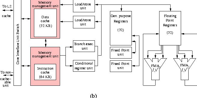
In many ways the POWER4+ processor core is similar to the former POWER3 processor: there are 2 integer functional units instead of 3 (called Fixed Point Units by IBM) and instead of a fused Branch/Dispatch Unit, the POWER4 core has a separate Branch and Conditional Register Unit, 8 execution units in all. Oddly, the instruction cache is two times larger than the data cache (64 KB direct-mapped vs. 32 KB two-way set associative, respectively) and all execution units have instruction queues associated with them that enables the out-of-order processing of up to 200 instructions in various stages. Having so may instructions simultaneously in flight calls for very sophisticated branch prediction facilities. Instructions are fetched from the Instruction Cache under control of the Instruction Fetch Address Register which in turn is influenced by the branch predict logic. This consists of a local and a global Branch History Table (BHT), each with 16 K entries and a so-called selector table which keeps track of which of the BHTs has functioned best in a particular case in order to select the prediction priority of the BHTs for similar cases coming up.
Unlike in the POWER3, the fixed point units performs integer arithmetic operations that can complete in one cycle as well as multi-cycle operations like integer multiply and divide. There are no separate floating-point units for operations that require many cycles like divisions and square roots. All floating-point operations are taken care of in the FP units and, like in the HP PA-8800, there is an instruction to accommodate the axpy operation, called Fused Multiply Add (FMA) at IBM's which could deliver 2 floating-point results every cycle. This brings the theoretical peak performance at 7.6 Gflop/s at the current clock frequency. Like in the HP processor, the composition of the floating-point operations should be such that the units have indeed enough FMAs to perform otherwise the performance drops by a factor of 2.
Although here the dual core version of the chip is described that is positioned for general processing, also a single core version is marketed that is recommended for HPC use. The reason is that in this case the bandwidth from the L2 cache does not have to be shared between the CPUs and a contention-free transfer of up to 108.8 GB/s can be achieved while in the dual core version a peak bandwidth of 163.2 GB/s is to be shared between both CPUs.
It is interesting to see that presently three vendors (AMD, Compaq, and
IBM) have facilities that enable glueless coupling of processors
although the packaging and implementation is somewhat different. All
implementations allow for low-latency SMP nodes with a considerable
number of processors stimulating the trend to build parallel systems
based on SMP nodes.